Technical features

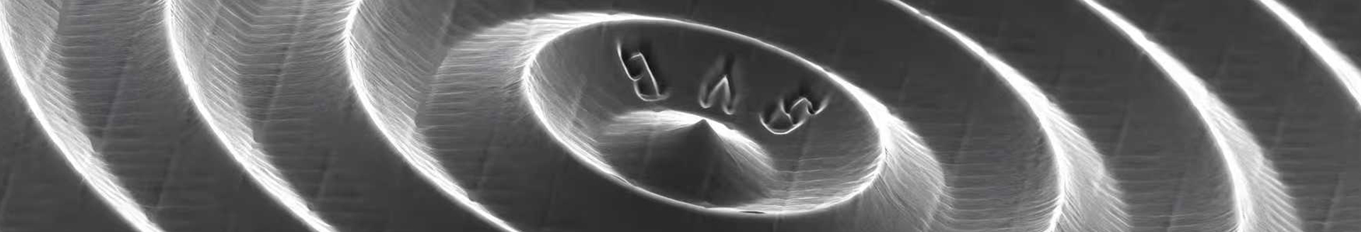
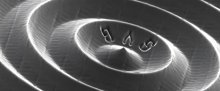
- Nanocrystal is a maskless lithography system specially designed for the fabrication of nano optical structures. It is equipped with a phase interference system with continuously variable spatial frequency to enable the fabrication of sub-wavelength optical structures with sub-nanometer modulation precision.
- The lithography system adopts a 355 nm ultraviolet light source, an interferometric optical system with a large numerical aperture (NA=0.9), and a field of view (FOV) with a pixel size of 100 micron for the fabrication of micro/nano optical structures in the 150 nm - 5 ІЬm range. It is equipped with 3D navigation focusing and high speed in-flight exposure mode, and is a good method for fabricating large-area sub-wavelength structures.It can be applied to the research of photonic crystals, diffractive optical elements, light field modulation displays, and optical metasurfaces, and fabrication of relevant devices.
Specifications

* The metrics may vary depending on the processes
Example applications


